Researchers at the University of California, Berkeley, and the Lawrence Berkeley National Laboratory have succeeded in fabricating mechanically flexible imagers using nanotube-based active-matrix backplanes. The devices, which can image in both the visible and X-ray range, could be used to make large-area flexible sensor networks for a variety of imaging applications, such as interactive surfaces and displays that can be pasted onto a host of surfaces and objects. The devices that work in the X-ray part of the spectrum might find use in portable medical imaging too.
Nanotube thin film transistors are ideal for making low-power active matrix backplanes on a wide range of substrates, including mechanically flexible plastics. Indeed, researchers have already managed to combine such backplanes with pressure sensors to make electronic “skins”, and with organic light-emitting diodes for flexible displays.
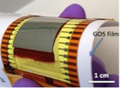
The team, led by Ali Javey, has now exploited these backplanes in another important application: large-area flexible imagers. The researchers made their devices by monolithically integrating organic photodetectors (OPDs) atop a nanotube backplane comprising an 18 x 18 pixel array. The actual size of the array is 2 x 1.5 cm.
Javey and colleagues chose OPD materials that respond to visible light for optical imaging applications. By adding a scintillator film (capable of converting incident X-rays into visible photons that are then detected by the OPDs) on top of the imager, they were also able to fabricate an X-ray light detector.
“The nanotube backplane consists of thin film transistors (TFTs) made using solution-processed semiconductor-enriched carbon nanotubes,” explains team member Zhibin Yu. “Such transistors have high mobilities of up to 50 cm2/V.s and high on-off current ratios of 106,” he told nanotechweb.org. “These values represent a significant advantage over silicon- and organic semiconductor-based devices that often have mobilities two orders of magnitude lower.”
The large-area visible light imager might be used as a new platform to develop interactive surfaces that can be laminated onto a variety of different surfaces, such as flexible plastics, and that can spatially map hand and body movements, he added. The flexible X-ray detector, for its part, might come in handy as a portable X-ray device for medical imaging applications.
The team says that it will now try to integrate a microlens array onto the pixels in its device for tuning light focus depth and increasing the sharpness of the images obtained.